


IC test board for Infineon
Easca manufactures Semiconductor Test Board, IC Validation Board and Power Semiconductor Test Board for semiconductor and power electronics customers.
Each Semiconductor Test Board supports high-layer-count stackup and controlled impedance, and every Semiconductor Test Board passes flying-probe testing.
The IC Validation Board covers socket interface, clock and load board designs, and each IC Validation Board is delivered with complete test documentation.
The Power Semiconductor Test Board handles high-current and high-voltage designs, with heavy copper up to 6 oz on each Power Semiconductor Test Board.
Applications: Semiconductor Test Board for ATE platforms, IC Validation Board for chip bring-up, Power Semiconductor Test Board for IGBT and MOSFET evaluation.
All Semiconductor Test Board, IC Validation Board and Power Semiconductor Test Board products are made in our ISO9001 certified factory.
OEM/ODM: custom Semiconductor Test Board, IC Validation Board and Power Semiconductor Test Board from design review to mass production.
Contact Easca for quotes and lead times on Semiconductor Test Board, IC Validation Board and Power Semiconductor Test Board.
Samples of Semiconductor Test Board, IC Validation Board and Power Semiconductor Test Board are available for evaluation.
Our engineering team supports stackup design, impedance control and DFM review at the quotation stage.
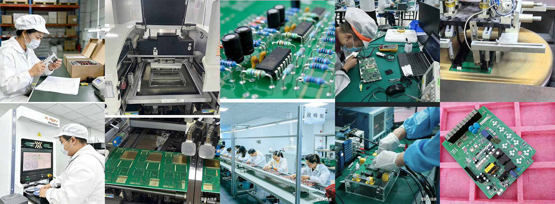
SMT Chip Mounting (Surface Mount Technology)
Solder Paste Printing: fabricate stepped stencils, large-size stencils, and other precision stencils to accurately print solder paste onto PCB pads via stencils.
Component Placement: Equipped with 6 YAMAHA high-speed placement lines, canachieve a daily output of over 15 million points.
Reflow Soldering: 10-zone reflow soldering equipment
DIP Insertion (Through-Hole Technology)
- Large-size components (e.g., electrolytic capacitors, connectors) are installed manually or via automatic insertion machines.
- Wave Soldering: selective wave soldering machines and conventional wave soldering pots.
Testing and Inspection:Visual Inspection,AOI,SPI,ICT,FCT,Aging Test
Material Management
- The customer’s original BOM is 100% cross-checked twice by two personnel to avoid wrong material usage and reverse polarity issues.
- Components stored in a moisture-proof environment (humidity < 30%).
- Solder paste in accordance with the IPC-J-STD-004 standard to prevent oxidation and failure
Contact us