


Photocell PCBA for ABB lighting device
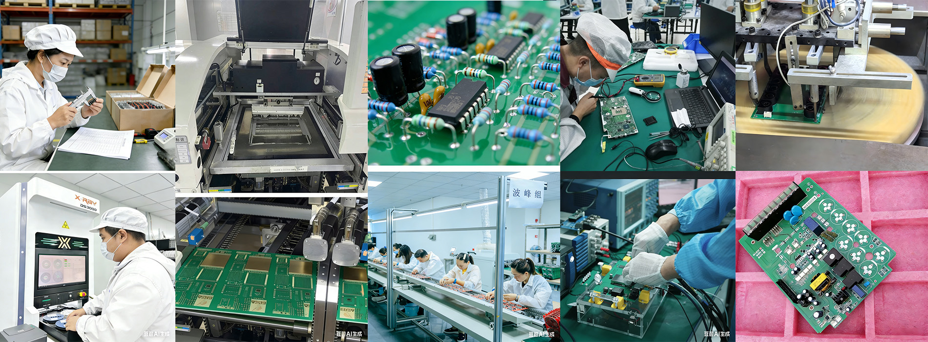
Easca is committed to PCBA prototype assembly as well as small-to-medium batch SMT chip mounting, DIP insertion, post-welding, testing, and assembly, along with PCB production andSMT precision stencilfabrication. We provide full-set PCBA processing services that meet the requirements of high precision, high difficulty, and superior quality! Our main PCBA product sectors include: medical, military, industrial, communication, and civil applications.
Easca PCBA Processing Core Processes
SMT Chip Mounting (Surface Mount Technology)
Solder Paste Printing: fabricate stepped stencils, large-size stencils, and other precision stencils to accurately print solder paste onto PCB pads via stencils.
Component Placement: Equipped with 6 YAMAHA high-speed placement lines, canachieve a daily output of over 15 million points.
Reflow Soldering: 10-zone reflow soldering equipment
DIP Insertion (Through-Hole Technology)
- Large-size components (e.g., electrolytic capacitors, connectors) are installed manually or via automatic insertion machines.
- Wave Soldering: selective wave soldering machines and conventional wave soldering pots.
Testing and Inspection:Visual Inspection,AOI,SPI,ICT,FCT,Aging Test
Material Management
- The customer’s original BOM is 100% cross-checked twice by two personnel to avoid wrong material usage and reverse polarity issues.
- Components stored in a moisture-proof environment (humidity < 30%).
- Solder paste in accordance with the IPC-J-STD-004 standard to prevent oxidation and failure
Process Optimization
- All stencils are designed with anti-solder ball features.
- Large-size sensitive components, such as electrolytic capacitors and relays, are pre-baked before reflow soldering.
- For PCBs with large-area blank pads or individual pads that will be bonded with components later, protective tape is applied before soldering to prevent scratches or solder adhesion.
Contact us